

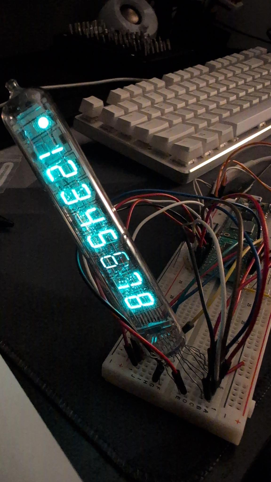
VFD Display Tube Code - Clock
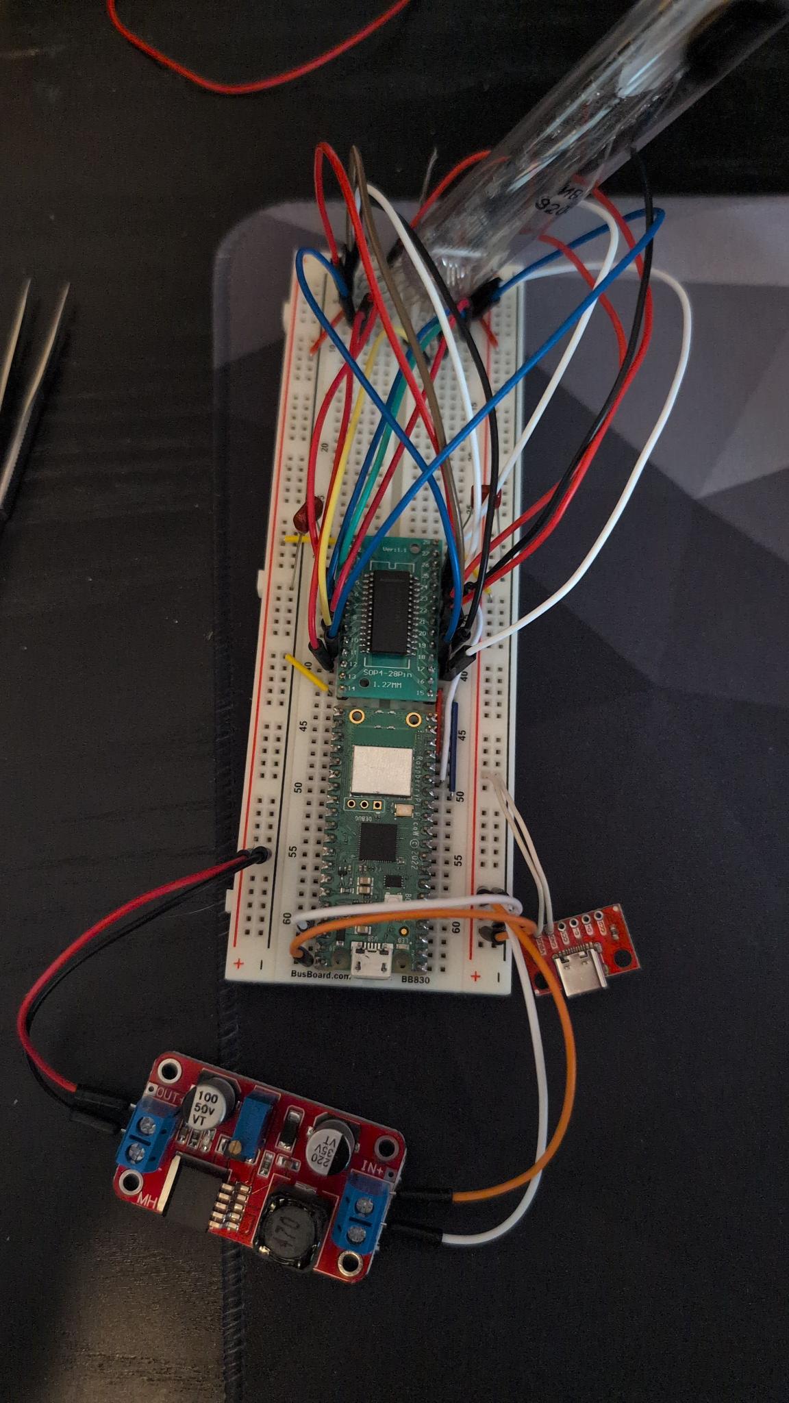
Overview This project demonstrates how to drive a VFD (Vacuum Fluorescent Display) using a Raspberry Pi Pico W and the MAXIM MAX6921AWI chip. The display setup includes a 7-segment display with a decimal point and 8 grids, controlled using a 20-bit buffer, leaving room for additional control logic. The VFD of choice this time around is the Soviet (Sovtek) IV-18 a.k.a ИВ-18 (Совтек).
Pin Mapping and Layout
Mapping Layout
- Display Details:
- The display consists of a 7-segment display + 1 dot (decimal point).
- There are
89 grids (digits), requiring1617 pins for control (8 segment pins +89 grid pins). - Only one grid pin is active high at a time, leaving
43 unused bits, which can be reserved for future use.
- Pin Mapping:
- Pins 0–7: Drive the segments (7-segment + dot).
- Pins 8–16: Control the grids (digits).
- Buffer Details:
- This setup uses 2 bytes + 1 bit (
1617 bits), but the MAXIM MAX6921AWI chip requires 20 bits. - The
43 remaining bits can be padded or reserved for control logic. - The chip’s clear pin can be triggered via the Pico, potentially using the last 4 output pins.
Voltage Note: Driving the clear pin requires careful consideration of the bus voltage (e.g., 25V for IV-18). A resistor ladder can step down voltages if needed.
- This setup uses 2 bytes + 1 bit (
VFD Segment Display Matrix
Physical VFD Pin Mapping:
 --         <- Top segment (Pin 12)
|  |        <- Left (Pin 11) and Right (Pin 10) middle segments
 --         <- Middle segment (Pin 9)
|  |        <- Left (Pin 5) and Right (Pin 4) bottom segments
 -- .       <- Bottom segment (Pin 3) and decimal point (Pin 2)
Logical Segment Mapping (A–H):
 --         <- Segment A (Top)
|  |        <- Segments F (Left) and B (Right)
 --         <- Segment G (Middle)
|  |        <- Segments E (Left) and C (Right)
 -- .       <- Segment D (Bottom) and H (Decimal point)
Alphanumeric Segment Pinout:
| VFD Pin | Segment |
|---------|---------|
| Pin 12  | A       |
| Pin 11  | F       |
| Pin 10  | B       |
| Pin 9   | G       |
| Pin 5   | E       |
| Pin 4   | C       |
| Pin 3   | D       |
| Pin 2   | H (Decimal Point) |
| Pin 1, 13 | Heating elements (not coded) |
Control Logic and Commands
The remaining 4 3 bits of the 20-bit buffer can be used for control logic. Here is the mapping of the control bits:
Control Bits Command Table
| Decimal | Binary | Hexadecimal | Command Description |
|---|---|---|---|
| 0 | 000 | 0x0 | N/A |
| 1 | 001 | 0x1 | N/A |
| 2 | 010 | 0x2 | N/A |
| 3 | 011 | 0x3 | N/A |
| 4 | 100 | 0x4 | N/A |
| 5 | 101 | 0x5 | N/A |
| 6 | 110 | 0x6 | N/A |
| 7 | 111 | 0x7 | N/A |
/*********************************************************************************
 * Authors: Aidan Bradley and Andrew Korman
 * Years: 2024-2025
 *
 * Description:
 * This program was written in C to drive a triode-based Vacuum Fluorescent Display
 * (VFD) system using the Maxim MAX6921 VFD driver chip. The code is designed for
 * use on the Raspberry Pi Pico microcontroller and utilizes the SPI interface to
 * communicate with the VFD chip. It implements real-time clock (RTC) functionality
 * for timekeeping and allows user interaction via button inputs for setting hours,
 * minutes, and seconds.
 *
 * Key Features:
 * - Real-time clock functionality for dynamic time display.
 * - Button-based input for adjusting time with debounce handling.
 * - SPI communication to drive the MAX6921 VFD chip.
 * - Seven-segment display formatting with control over segment illumination and
 *   grid selection.
 * - Modular and well-commented functions for initializing hardware, updating the
 *   VFD, and managing user input.
 *
 * Dependencies:
 * - Raspberry Pi Pico SDK
 * - Standard C libraries: stdio.h, string.h
 * - Hardware-specific libraries: pico/stdlib.h, hardware/spi.h, hardware/rtc.h
 *
 * Note:
 * This code assumes a specific hardware setup, including pin assignments for SPI,
 * latch, and button inputs. Ensure proper connections and configurations when
 * deploying this code.
 *
 * Disclaimer:
 * This code was developed by Aidan Bradley and Andrew Korman and is provided as-is.
 *********************************************************************************/


#include <stdio.h>
#include <string.h>
#include "pico/stdlib.h"
#include "pico/binary_info.h"
#include "hardware/spi.h"
#include "hardware/rtc.h"
#include "pico/util/datetime.h"

// Define pin connections
const uint SPI_D = 11; // MOSI (SPI TX)
const uint SPI_C = 10; // SCK (SPI Clock)
const uint SPI_L = 13; // Latch pin (GPIO)

const uint BPID1 = 16;  // Button 1 Pin ID
const uint BPID2 = 17;  // Button 2 Pin ID

// SPI configurations
#define SPI_PORT spi1 // Using SPI1 interface
#define SPI_BAUDRATE 2000000 // 2 MHz

// Segment control and grid control arrays
uint8_t segment_control[] = {
  0b00111111, // 0: A B C D E F
  0b00000110, // 1: B C
  0b01011011, // 2: A B D E G
  0b01001111, // 3: A B C D G
  0b01100110, // 4: B C F G
  0b01101101, // 5: A C D F G
  0b01111101, // 6: A C D E F G
  0b00000111, // 7: A B C
  0b01111111, // 8: A B C D E F G
  0b01101111,  // 9: A B C D F G
  0b10000000, // decimal: H (10)
  0b01000000, // dash: G (11)
  0b00000000  // blank (12)
};

uint16_t grid_control[] = {
  0b100000000, // grid 0 (decimal)
  0b010000000, // grid 1
  0b001000000, // grid 2
  0b000100000, // grid 3
  0b000010000, // grid 4
  0b000001000, // grid 5
  0b000000100, // grid 6
  0b000000010, // grid 7
  0b000000001  // grid 8
};

uint8_t state[9] = {
  12, // decimal
  12, // hourleft
  12, // hourright
  11, // dash
  12, // minleft
  12, // minright
  11, // dash
  12, // secleft
  12  // secright
};

// define global variables
uint8_t data[3];
uint8_t digit;
uint8_t grid;
uint32_t combined_data;
bool button_state[]={false, false};

// define datetime struct
datetime_t t = {
  .year  = 2000,
  .month = 06,
  .day   = 05,
  .dotw  = 5, // 0 is Sunday, so 5 is Friday
  .hour  = 01,
  .min   = 59,
  .sec   = 45
};

// function to update the vfd
void write_vfd(uint8_t digit, uint8_t grid) {
  combined_data = (grid_control[grid] << 8) | segment_control[digit];
  data[0] = (combined_data >> 16) & 0xFF;
  data[1] = (combined_data >> 8) & 0xFF;
  data[2] = combined_data & 0xFF;

  spi_write_blocking(SPI_PORT, data, 3);

  gpio_put(SPI_L, 1);
  sleep_us(1);
  gpio_put(SPI_L, 0);
}

void init_gpio(uint bpid1, uint bpid2){
  stdio_init_all(); // initial std i/o setup
  gpio_pull_down(bpid1);
  gpio_pull_down(bpid2);

  spi_init(SPI_PORT, SPI_BAUDRATE);
  gpio_set_function(SPI_C, GPIO_FUNC_SPI);
  gpio_set_function(SPI_D, GPIO_FUNC_SPI);

  gpio_init(SPI_L);
  gpio_set_dir(SPI_L, GPIO_OUT);
}

void double_debounce(uint GPIO1, uint GPIO2) {
  bool first1 = gpio_get(GPIO1);
  bool first2 = gpio_get(GPIO2);
  sleep_ms(1);
  bool second1 = gpio_get(GPIO1);
  bool second2 = gpio_get(GPIO2);
  if ((first1 && second1) && (first2 && second2)){
    button_state[0] = true;
    button_state[1] = true;
  }
  else if ((first1 && second1) && (!first2 && !second2)){
    button_state[0] = true;
    button_state[1] = false;
  } else if ((!first1 && !second1) && (first2 && second2)){
    button_state[0] = false;
    button_state[1] = true;
  } else {
    button_state[0] = false;
    button_state[1] = false;
  }
}

int main() {
  init_gpio(BPID1, BPID2);
  rtc_init();
  rtc_set_datetime(&t);
  sleep_ms(1000);

  uint8_t counter = 0;
  bool setmode = false;
  int setcode = 0;

  while (1) {
    double_debounce(BPID1, BPID2);
    if ((button_state[0]) && !setmode){
      setmode = true;
    } else if ((button_state[0]) && setmode) {
      if (setcode < 2){
        setcode += 1;
      } else if (setcode >= 2){
        setcode = 0;
        setmode = false;
      }
    }
    if ((button_state[1]) && setmode) {
      if ((setcode == 0) && (t.hour <= 23)){
        t.hour += 1;
      } else if ((setcode == 0) && (t.hour == 24)){
        t.hour = 0;
      }
      if ((setcode == 1) && (t.min <= 59)){
        t.min += 1;
      } else if ((setcode == 1) && (t.min == 60)) {
        t.min = 0;
      }
      if ((setcode == 2) && (t.sec <=59)){
        t.sec += 1;
      } else if ((setcode == 2) && (t.sec == 60)) {
        t.sec = 0;
      }
    }

    rtc_get_datetime(&t);

    if (t.hour >= 12) {
      state[0] = 10;
    } else {
      state[0] = 12;
    }

    if ((t.hour == 0) && (!setmode)) {
      t.hour = 12;
    }
    else if (t.hour > 12) {
      t.hour -= 12;
    }

    if (t.hour < 10) {
      state[1] = 12;
    }
    else {
      state[1] = (t.hour / 10);
    }

    state[2] = (t.hour % 10);
    state[4] = (t.min / 10);
    state[5] = (t.min % 10);
    state[7] = (t.sec / 10);
    state[8] = (t.sec % 10);

    write_vfd(state[counter], counter);

    counter ++;
    if (counter == 9) {
      counter = 0;
    }
    sleep_us(1500);
  }
}
- Sending data via SPI to the Maxim chip requires the data to be loaded backwards, hence sending the high byte first
- Data separately to that, the data must be sent LSB style via SPI, which was taken care of by swapping the order of the predefined segment and grid code
- With the data flipped appropriately, and the byte order sent backwards, we achieve intercommunication with the VFD driver chip
- Data segments are 0-9, so you must reverse them 9-0. Grid segments are the same. It should read PADDING + GRIDCONT + SEGMCONT => CONTR-SEQ
- CONTR-SEQ is split into three bytes, then sent VIA SPI bus.
- SPI does not have a 3rd wire, but since the maxim chip does not display any output until the latch pin is triggered, we added a 3rd pin for sending a latch signal to. It is pretty fast, so 1 microsecond was used as a buffer between setting it high and then back to low